
PCL
PCL
Planar Carbon Lattices
RTG-2861-PCL
B1 - Self-assembled device structures and unique PCL-structures
Principal investigator: Prof. Dr. Marcus Halik, FAU Erlangen, [webpage]
Doctoral researcher in the 1st cohort: Jiwon Byun
Doctoral researcher in the 2nd cohort: Marie Kaiser
PCLs in larger scale systems still lacks in proper methodology to position them appropriately in controlled 2D and 3D setups. A chemical guidance system would enable PCLs (i) to grow selectively on place or (ii) to self-assemble flakes with precise control on area coverage, (iii) to promote defined 2D-stacking, and (iv) to efficiently interact with other devices components. Non-conventional 2D materials (e.g. self-assembled monolayers, SAMs, and double layers) provide specific environment with precisely controlled molecular dimensionality and wide chemical composition.[1] Double-layers on nanoparticles can be selectively “loaded” and provide pocket features, which could enable unusual conversion of reactants by (i) confined space conditions, (ii) e.g. photonic, or (iii) electrochemical activation or (iv) lead to unusual PCLs.[2]
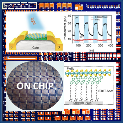
Figure: Wafer-scale SAM-MoS2 photo-junctions with chip layout as background.[3]
Thesis topic 1st cohort: Devices of PCLs grown on SAMs
We will develop and provide a toolbox of SAMs to control selective deposition/ growth of 2D materials (PCLs, TMCs, MOFs π-SAMs) (Dong, Kaskel) in devices (junctions, transistors, memories). Therefore, pure and mixed as well as pre-patterned features (based on different SAM molecular fashion) will be implemented on corresponding device platforms on wafer scale.
Thesis topic 2nd cohort: SAM-PCL heterojunctions – control of interlayer “communication”
[2] N. Wang, Y. Zhi, Y. Wei, W. Zhang, Z. Liu, J. Huang, T. Sun, S. Xu, S. Lin, Y. He, A. Zheng, Z. Liu, Nat. Commun. 2020, 11, 1079.
[3] B. Zhao, Z. Gan, M. Johnson, E. Najafidehaghani, T. Rejek, A. George, R. Fink, A. Turchanin, M. Halik “2D van der Waals Heterojunction of Organic and Inorganic Monolayers for High Responsivity Phototransistors”, Advanced Functional Materials, 2021, 2105444.